pslab-mini-hardware: the open design files behind the PSLab Mini
PSLab Mini Hardware https://pslab.io
At a glance
- What is it?
- This repository holds the board design files for the PSLab Mini, a pocket instrument that combines an oscilloscope, a logic analyser and a multimeter around an STM32H563 and an ESP32C3. It is a hardware project, so what you get is schematics and a bill of materials, not a library you install.
- Who is it for?
- Adopt this design if you want a three-instrument board you can study, build, or modify, and you are comfortable reading schematics and ordering parts by hand. Do not adopt it if you need a finished, certified instrument or a working software stack on day one, since the firmware lives in a separate repository and the board is a design under development.
- Can I use it commercially?
- Yes. Apache-2.0 is a permissive licence: you can use, modify and sell software built on it, as long as you keep its copyright and licence notices.
- Is it still maintained?
- Yes. The repository last received commits 75 days ago.
- What is it written in?
- GitHub does not report a main language for this repository.
Answers come from the project's GitHub data, last synced on November 7, 2026, and from our analysis. They are not legal advice.
Star history
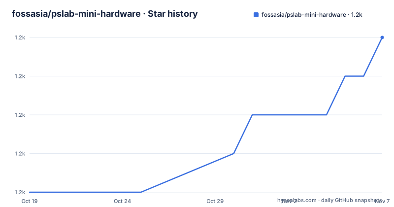
- fossasia/pslab-mini-hardware1,229 ★ · +4
| Repository | 2026-10-19 | 2026-11-07 |
|---|---|---|
| fossasia/pslab-mini-hardware | 1.2k | 1.2k |
4 Stars in the last 19 days, measured from the daily GitHub snapshot. Compare with other projects
Editorial analysis
One board that packs three instruments instead of one
The PSLab Mini is described in the README as a scaled-down version of the PSLab board, aimed at providing instruments for signal measurements. Rather than one specialised function, it folds three into a single PCB: an oscilloscope, a logic analyser and a multimeter.
The headline numbers are on the oscilloscope side. Two channels, a 12-bit ADC running at 5MSPS, and BNC connectors so ordinary scope probes plug straight into the board. The README also states that the sampling rate is higher than that of the current PSLab board, which is the clearest statement in the project about how the Mini differs from its full-size sibling.
The logic analyser is narrower by design, offering two channels, and the multimeter covers AC and DC voltage, resistance, capacitance and frequency. For a student, a lab teaching assistant, or a hobbyist, that combination removes the need to own three boxes, and the open design files let you build the board yourself rather than buy one.
What you cannot get from this repository is a working instrument out of the box. The firmware for the board lives at fossasia/pslab-mini-firmware, and this repository is the hardware side of the project.
Two microcontrollers share the board and the reset button
The architecture is a main microcontroller paired with a secondary one that adds wireless connectivity. The main chip is an STM32H563RIT6, the secondary chip an ESP32C3, and the README says the ESP is integrated in conjunction with the STM32 to enable wireless connectivity via the board.
The two chips talk to each other over dedicated buses. One UART and one SPI line are used for the interface between the ESP32 and the STM32, so the connection between them is not sharing bandwidth with anything else.
Reset behaviour is handled for you. The reset button on the board resets both the STM32 and the ESP32 at the same time, and the STM32 can additionally reset the ESP32 through an output pin, described in the README as:
`PB5` (STM32) → `CHIP_EN` (ESP32)That single line matters more than it looks. It means a host program talking to the ESP32 can force a clean restart of the wireless side without the user pressing anything, which is the kind of detail that decides whether a board behaves well in an automated measurement script or needs a human nearby.
The design goal recorded in the README is compactness and manufacturability, with all components placed on one PCB side.
Signal routing: oscilloscope on PA0 and PA1, instruments on their own pins
The README publishes a full pinout, which is the most useful part of the document for anyone reproducing the board. The oscilloscope channels land on the analogue pins PA0 and PA1, one BNC connector each, and the analogue pins PA5, PA6, PA7, PC4, PC5 and PB0 are also listed as analogue, with the digital pins PC8, PC9 and PA8 available as general digital inputs.
The measurement functions each claim a dedicated pin, so the multiplexer and the analogue front end do not have to share a channel:
|LA1|PA3|Logic Analyser Channel-1|
|LA2|PA2|Logic Analyser Channel-2|
|FQY|PA4|Frequency Measurement|
|VOL|PC0|Voltage Measurement|
|RES|PC1|Resistance Measurement|
|CAP|PC3|Capacitance Measurement|
Two op-amps appear in the parts list and they are not interchangeable roles. The OPA356AIDBVR is a single channel high-speed CMOS op-amp, and the TLV9001IDCK is a single channel low-speed CMOS op-amp, which suggests a fast path for the scope channels and a slower path for the slower measurement functions. The README does not describe the analogue signal path in detail, so how each amplifier is wired is left to the schematic in the schematic/ directory.
The bus segregation is also explicit. Of the two UARTs, two SPIs and one I2C exposed from the STM32 pinout, one UART and one SPI are consumed by the ESP32 link, and the remaining UART, SPI and I2C are brought out to external headers.
Building the firmware and flashing it in two stages
There is no package manager here, and the README contains no make targets or shell commands to copy. The project states the toolchain and the two programming routes instead.
Firmware is compiled with the open ARM toolchain, listed in the README as the compiler gcc-arm-none-eabi, and the development environment references the HAL and LL documentation for the STM32H5 family. Flashing is split in two, and the README describes the split like this:
  * For uploading the bootloader onto the board: [STLink](https://www.st.com/en/development-tools/st-link-v2.html)/Any other ARM programmer
  * For uploading the firmware onto the board: Directly using USB ([OpenBLT](https://github.com/feaser/openblt) bootloader is already present on the board)
Read that as a one-time step and a repeated step. The bootloader goes on once through an STLink or any other ARM programmer, and because the OpenBLT bootloader is already present on the board, later firmware updates go straight over USB. That is the difference between a board you can iterate on and a board that needs a debug probe on the bench every time.
The firmware source itself is not in this repository. The README points to fossasia/pslab-mini-firmware, so getting the software side working is a separate checkout, and the pin names documented here are the contract between the two.
The enclosure is a stock Raspberry Pi 3 and 4 case
The mechanical design is unusually pragmatic. The PSLab Mini is designed to use Raspberry Pi 3 and 4 cases, which the README says are already widely available and need no modification, and it adds that all the ports remain accessible in the casing: USB, the BNC connectors and the battery connector.
That removes the most annoying part of building an instrument. A custom enclosure means a custom 3D print, a supplier, or a slot of evenings with a modelling tool, and the port cutouts alone are the fiddly part. With a Raspberry Pi case, the fit is already there and the connector positions are already correct. The prototype photographs in docs/images/ show the board sitting in such a case.
The battery connector in that list is worth noting, because the parts list includes an IP5189T battery management chip alongside the AMS1117-3.3 buck regulator that steps 5 V down to 3.3 V and an MT2496 inverting buck converter that produces minus 2 V. A negative rail is not something a USB powered design needs, and it points to a front end that needs a bipolar supply. The README does not describe the power budget, so how long the board runs on a charge is not something the project states.
What the board does not give you
The bill of materials is short and readable, and the constraints are easier to spot than the features. There is one ESP32C3 and one STM32H563RIT6, two op-amps, and a 32 megabit, 4 megabyte W25Q32JV NOR flash attached to the ESP32 over SPI_1 for the wireless side. Resistances and capacitors are listed as assorted, which means the schematic is where the real component count lives.
Two limits stand out. First, the external header budget is thin: one UART, one SPI and one I2C reach the outside, because the second UART and second SPI are already committed to the ESP32 link. A project that needs two I2C buses or several serial peripherals has to re-spin the board rather than plug in a converter.
Second, the flexibility of the ESP32C3 is bought with board area and power, and this design pays both. The README does not state an idle or active power figure, so battery life is a question you would have to answer by measuring the board rather than by reading the project.
Finally, this repository is hardware design files. The top level contains .github/, docs/, output/, and schematic/, with no application code, no simulation model, and no test suite for a firmware image. If your goal is to measure signals from Python tomorrow, the board design is the wrong level of abstraction.
Licence, activity and the shape of the contribution
The project is released under the Apache 2.0 licence, and the repository carries a LICENSE file. That is a permissive licence with an explicit patent grant and a notice condition, so a derived board design can be released under different terms as long as the licence text and notices travel with it. Reading a licence is not legal advice, and a commercial product based on the design deserves a proper review.
The repository is not archived and the last push was on 2026-08-24, so the design is still moving. It also has no GitHub releases, which for hardware is not surprising: there is no versioned artefact to download, and the artefacts are the schematic files, the board layout, and the rendered output under output/.
The contribution surface is narrow and specific. Contributors work with the schematic sources, the design goals in the README, and the open firmware repository that consumes the pin assignments. A useful contribution therefore points at a specific electrical decision, such as a protection part, a rail, or a connector change, and the fastest way to check whether a proposal is welcome is to read the pinout section and the parts list and see whether the change touches an already fixed interface.
Editorial conclusion
Adopt this design if you want a three-instrument board you can study, build, or modify, and you are comfortable reading schematics and ordering parts by hand. Do not adopt it if you need a finished, certified instrument or a working software stack on day one, since the firmware lives in a separate repository and the board is a design under development. Before starting, check the schematic/ and docs/ directories against your own requirements, confirm the flash, battery and regulator parts listed in the bill of materials are still orderable, and decide early whether the ESP32C3 link is worth the extra board area.
Frequently asked questions
What instruments does the PSLab Mini provide?
The board combines a two channel oscilloscope with a 12-bit ADC at 5MSPS, a two channel logic analyser, and a multimeter that measures AC and DC voltage, resistance, capacitance and frequency. The oscilloscope channels use BNC connectors for probes.
How do I flash firmware onto the PSLab Mini?
The bootloader is uploaded once with an STLink or any other ARM programmer, and firmware updates afterwards go directly over USB because the OpenBLT bootloader is already present on the board. The firmware source itself lives in the separate pslab-mini-firmware repository.
Which microcontrollers does the PSLab Mini use and what connects them?
The main microcontroller is an STM32H563RIT6 and the secondary one is an ESP32C3 for wireless connectivity. One UART and one SPI line are used between the two chips, and the reset button resets both of them at the same time.
Can I attach peripheral devices to the PSLab Mini headers?
The external headers expose one UART, one SPI and one I2C, taken from the STM32 pinout. The remaining UART and SPI are already used for the link between the STM32 and the ESP32.
Official sources
Add this badge to your README
If you maintain this project, the badge below links readers to this analysis and shows its maintenance status from the daily GitHub snapshot. Paste the markdown into your README; add ?metric=license or ?metric=stars to the image URL for a different field.

[](https://hysenlabs.com/projects/fossasia-pslab-mini-hardware)Star history chart for your README
[](https://hysenlabs.com/projects/fossasia-pslab-mini-hardware)Was this useful?